Antistatic Tape and Label Materials For Optoelectronic Devices.
UltraTape makes antistatic tapes and label materials with static dissipative surface resistances and low tribocharging pressure sensitive adhesives (PSA) that allow them to protect static sensitive optoelectronic devices such as LED’s, photo and laser diodes, solar cells, etc. and help prevent harmful electrostatic discharge (ESD) events.
UltraTape has introduced a variety of antistatic single and double coated engineered tapes and high performance label materials aimed at protecting static sensitive optoelectronic devices. These new materials offer both static dissipative features that safely dissipate triboelectric charges as well as low tribocharging PSAs that provide low peel voltages when their liners are removed.
Optoelectronics, being semiconductor based devices, are highly susceptible to current spikes. These spikes result from electrostatic discharges (ESD) essentially high voltage, large joule discharges occurring over very short time frames. The resulting damage caused by these ESD events can be detected during manufacturing and/or during testing and can even remain latent and fail during operation by an end user. This increases the cost of manufacturing as well as warranty costs, plus can present legal liabilities if harm comes to an end user.
Triboelectric charges can occur via the human body model (HBM) when a human comes in contact with the device. Charging of the device can also occur when it comes in contact with other devices in the manufacturing environment. This type of charging is called charge device model (CDM) and includes contact with pick and place robots, transfer and conveyor mechanisms, fixturing, etc. Both forms of charging are prevalent in optoelectronic device manufacturing, both can lead to damaging ESD events and Polyonics antistatic materials can help solve both situations.
Our tapes are manufactured including a variety of specially formulated conductive elements that help prevent damaging ESD events. The conductive elements provide surface resistances of 10^5 to 10^9 Ohms, the heart of the dissipative spectrum. This unique feature allows the materials to safely dissipate triboelectric charges and prevent ESD events. In addition, the materials include low tribocharging PSAs that produce a low peel voltage of <100v, when their liners are removed further protecting the optoelectronic device during application or removal.
The potential for damage from electrostatic discharges depends on charge density and how charges are handled by the surfaces they reside on. Spots of charge (high charge densities) persist on insulative surfaces for long periods of time with little or no charge dissipation. If left unchecked, these spots can continue to grow in strength and, if contacted by a ground, can result in damaging ESD events. Conductive surfaces dissipate electrostatic charges rapidly which can cause electrical shorts and expose electrical components and devices to higher than expected voltages.
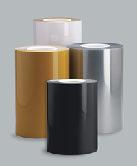
UltraTape’s antistatic materials are also designed to survive extreme temperatures and exposure to harsh chemicals during manufacturing. These materials include high performance antistatic label materials, used for tracking static sensitive devices along with single and double coated engineered tapes. The antistatic single coated polyimide tapes can be used for masking, protecting, insulating and isolating. The single coated tape is both antistatic and flame retardant.
The double coated antistatic polyimide tapes and antistatic PET tape are used for bonding applications involving static sensitive devices. High opacity single and double coated antistatic tapes are also available when, in addition to protecting static sensitive devices, the management of light (masking, blacking, dispersing, etc.) is required.
We also manufacture antistatic polyimide label materials for printed circuit board tracking applications as well as polyester label materials for electronic component identification. All materials can be thermal transfer printed and are designed to meet and/or exceed the high temperature requirements of the reflow and wave solder environments in the PCB manufacturing process.