Thermal Slide debonding for temporary bonding processes
April 9, 2013 Brewer Science blog
Thermal slide debonding represents the next significant advancement in obtaining high-yield thin wafer results. Initial detection of anomalies and cracks usually occurs during debonding; however, many causes for this damage originate during upstream bonding material coating, curing, bonding, and thinning processes. Moreover, only thermal separation tools that are highly precise and highly accurate will consistently render desirable process yields. The bonded pair is subjected to many thermal and compressive forces during processing and debonding. The thinned device layers are often very sensitive to outside factors including temperature, vacuum, and mechanical compression and release.
For debonding, relatively speaking, silicon materials are inherently more flexible than III-V compounds and allow greater control tolerances. Consequently compound semiconductor (CS) materials require significantly tighter control of platen temperature uniformity, pull force, vacuum fluctuations, platen separation, and platen co-planarity. The Cee® 1300CSX thermal slide debonder (see image below) has been specifically designed to meet and exceed these specifications.
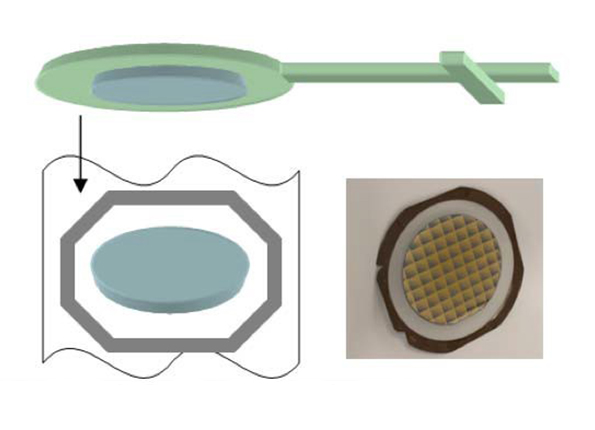
In this tool, wafer stacks are processed with the thinned device wafer orientated to contact the upper chuck and the carrier substrate is held in place by a vacuum emanating from the lower chuck. A manual insertion tool accurately aligns the bonded pair onto the lower platen lift pins. The lift pins are programmed electronically and provide precisely controlled acceleration for bringing the substrate to the desired set point temperature for heating the thermoplastic bonding material to the appropriate temperature to achieve a viscosity of < 300 Pa·s. The following steps outline the standard process flow for thermal separation (see diagram below).
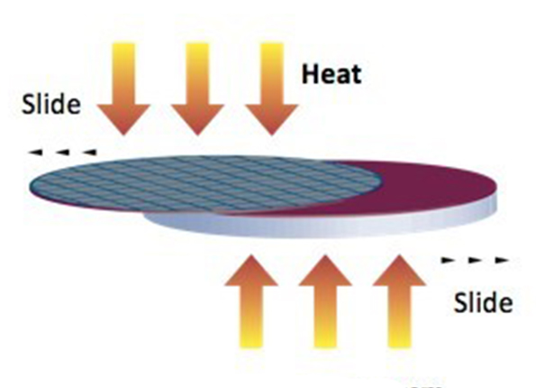
Thermal slide diagram
Operating the debonder involves the following processing steps:
- Load the debonding recipe (platen temperatures, pull force, thermal dwell times, electronic lift pin (ELP) positions, platen positional search windows, vacuum sensing threshold, etc.).
- Confirm the stack configuration (diameter and height/thickness). Recipes must match these physical characteristics.
- Using insertion tool, load the wafer onto the lift pins.
- Initiate the debonder recipe.
- The first recipe step is adjusting the lift pin positional height to allow a gradual increase in temperature for thermally sensitive materials.
- After achieving the appropriate thermal stabilization, the pre-bake step concludes, and the lower platen moves from the load to the press position.
- Upon reaching the press position, the platen is raised to the appropriate height to a predetermined vacuum search position.
- Once the minimum vacuum threshold is achieved, the system will enter the thermal stabilization step to ensure minimal temperature gradients.
- After the minimum temperature gradient is reached, the lower platen will pull in the x direction within preprogrammed force and speed limitations. During this pull, the following variables are monitored, controlled, and logged: z position, x position, force, speeds, upper and lower vacuum, upper and lower temperature, and process sampling time. The consistent profile of these variables is evidence of appropriate debonding parameters and may be used as a statistical process control.
- Upon debonding completion, the lower platen will drop and move to the load/unload position.
- The vacuum will shut off, and the lift pins will rise to the unload position for removal of the carrier.
- A specialized Gel-Pak® end effector is then inserted into tool under the upper platen and raised to a minimal distance (<2 mm) from the device wafer. Vacuum is released on the upper platen, and the wafer is gently transferred to the top surface of the Gel-Pak® end effector.
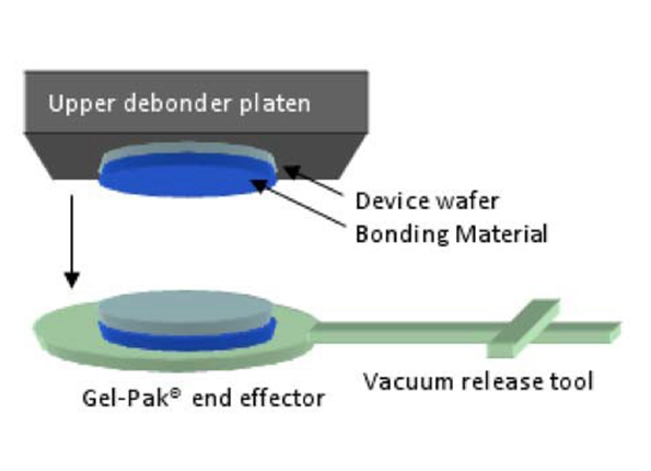
Removal of thinned device from upper platen using Gel-Pak® end effector
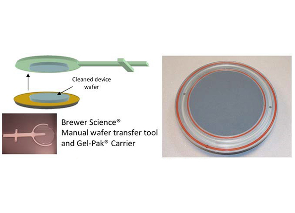
Transferring the intact device to a post-debonding spin-cleaning tool is the next critical step. The most common transfer method is outlined below:
- The device wafer and Gel-Pak® end effector are removed using the extraction tool assembly, and the entire Gel-Pak®/thinned device wafer structure is flipped onto a full sized porous ceramic spin chuck. Vacuum is applied through the spin chuck, and the device is released from the Gel-Pak® layer for cleaning.
- The remaining bonding material is removed from the device in a spin-cleaning process similar to a stream-puddle develop process. Megasonic cleaning is also a popular, safe method for cleaning residual bonding material to decrease cycle times and reduce solvent consumption (see photo below).
- After being cleaned, the device is lifted from the spin chuck with another clean Gel-Pak® carrier and mounted to a film frame on dicing tape.
Gel-Pak® transfer to porous ceramic spin chuck
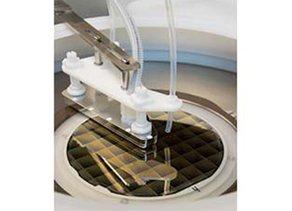
Megasonic cleaning on film frame
Device wafer transferred from Gel-Pak® (carrier) to film frame
We suggest using two different wafer transfer tools: one for transferring wafer that still has bonding material (Steps 1 & 2) and the second for transferring clean wafer (Steps 3 & 4)
Brewer Science is a registered trademark of Brewer Science, Inc.