Fixing the Bane of Costly Component Out Of Pocket Defects
The march of technological prog ress continues as traditionally bulky and discrete microwave devices become integrated in increasinglysmaller microelectronic modules and packages. New high performance GaN, GaAs, InP and other Class III-V and silicon semiconductor devices, along with high performance silicon variations such as SiC, are designed to push performance and enable new communications and sensing applications. As examples, active electronically scanned array radar and long-range, high throughput unmanned aerial vehicle telemetry are possible due to advances in RFICs and MMICs. As with most advancements in technology, the steps forward come with design challenges.
These challenges may be unknown and impossible to predict until the devices are shipped and integrated in new assemblies and systems. Often, enhanced features, integrated capabilities and heightened performance make the semiconductor die more expensive, and the loss of any die becomes a significant issue. This has been the case for a new generation of thin compound semiconductor die. BAE Systems, a global aerospace and defense technology company, and GelPak, a division of Delphon, have investigated the loss of millions of dollars from “cost of poor quality incidents” caused by die migration in waffle pack trays, known as component out of pocket (COOP) defects.
Their study revealed that while die migration occurred during customer handling of the waffle packs and chip trays, a significant amount occurred during the packaging by the supplier and subsequent transit to the customer. The wide flatness tolerances between the tray and the lid of traditional waffle packs, which far exceed the thickness of the thin semiconductor die, was the principal culprit.
This article discusses the joint study between Gel-Pak and BAE Systems and the development of a Lid-Clip Super System (LCS2™) to reduce die migration. The LCS2 protects extremely thin die, down to 2 mils(50 μm), during the jostling which occurs during handling and transport by semiconductor manufacturers, their distributors and customers around the world.
REDUCING DIE THICKNESS
Organizations from DARPA to cellular operators have invested in advanced semiconductor processes to enhance the performance of RFICs and MMICs, performance advantages such as higher power density, higher frequency coverage with wider bandwidth, improved linearity, lower noise and more integration. These developments have led to more compact ICs while integrating more signal chain components and features on the same chip, created a system-onchip. These new processes operate through the microwave frequencies and into the mmWave spectrum, enabling new systems for communications, automotive, satellite and defense.
Lowering the cost, weight and size of the semiconductor devices helps to enable new systems. One aspect is reducing die thickness, which reduces the thermal resistance between the device junction and the conductive path that removes the heat. The RF performance may also benefit from thinner die, with lower parasitics that extend the upper frequency range. Thinning techniques have been developed for compound semiconductor and silicon on insulator wafers to reduce die thicknesses for RF, microwave and mmWave applications.
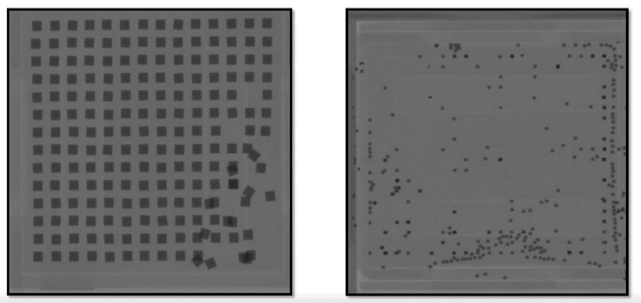
X-ray images of COOP with a traditional waffle pack.
DIE MIGRATION
Despite the performance and integration benefits, reducing die size causes handling and transportation challenges. COOP refers to a die in a waffle pack escaping its pocket, possibly moving to the pocket of another die (see Figure 1). This migration is inconvenient and costly. Die in the same pocket may become damaged as they bounce
and grind against each other. A die may flip, changing its orientation
and causing placement errors with automated handling equipment.
Die may become lodged between pockets, damaged by the waffle pack or migrate to another pocket when the waffle pack is opened.
COOP degrades the quality of the manufacturing process, causing
- Component damage and scrap
- Additional labor to inspect and reorder components
- Manufacturing delays from yield loss and interrupted production
- Reduced pick-and-place machine utilization
- Additional quality management administration
- Over-engineering the automated assembly process.
Die migration will increase manufacturing cost. Since the cost of MMICs and RFICs is substantial, losing even a few from COOP can add thousands of dollars from damage, scrap and non-value-added labor. The worst-case scenario occurs when a defect from migrated die is not caught until after die placement in the next higher assembly, adding the cost and delay for troubleshooting and rework.
ROOT CAUSE
Historically, the cause of die migration has been attributed to handling when opening the waffle pack, although there was little investigation of the end-to-end process of handling, packaging, storing and transporting semiconductor die. When traditional waffle pack chip trays were designed, die were thicker, i.e., hundreds of micrometers. In the late 2000s, die thickness began to shrink below 250 μm and is now in the tens of micrometers. Yet the industry made little change to die packaging practices for waffle packs, which increased COOP losses. Not surprisingly, device suppliers and their customers saw each other as the cause of the increasing problem. Use of X-ray and 3D measurement systems have led to more accurate identification of root causes, and there are many:
- Lack of awareness of Entegris’ literature describing warpage and the potential for migration
- Carbon loaded polypropylene lids and trays with a 0.012 in.warpage specification
- ABS and carbon loaded polycarbonate lids and trays with a 0.004 in. warpage specification
- Irregular deformation of lids and trays caused by the standard one-piece clip
- Non-woven polyethylene inserts misaligned and pinched during assembly, creating escape paths
- Components not flat in the chip tray before lidding
- Stacked components, i.e., two or more components in a single pocket due to operator error or warped lids
- Operator-dependent assembly process
- Application of label to bottom side of waffle tray by customers requires removal of the clip
- Worn or broken one-piece clip
- Bump lid failure from improper use and warpage.
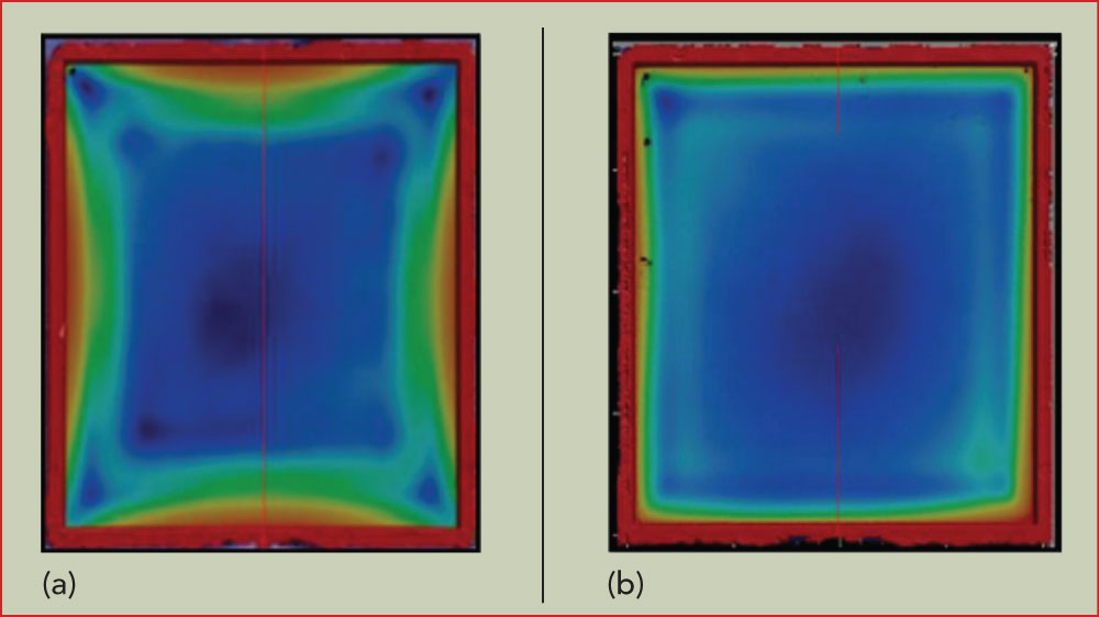
Fig. 2 - Measured internal surface flatness of carbon loaded polypropylene (a) and carbon loaded polycarbonate (b) lids.
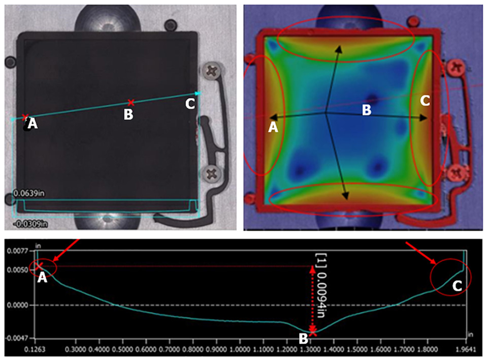
Fig. 3 - Measured internal lid surface flatness of the traditional waffle pack lid-clip system, showing 9.4 mil deflection between points A and B.
To improve the knowledge of COOP with the goal of reducing it, VJ Electronix developed an Xray counter system (XQuik II) for BAE Systems in 2017. The XQuik II can view and count the components within a sealed waffle pack during receiving inspection and identify COOP before the waffle pack is opened.
Data from the XQuik II system showed substantial levels of COOP when waffle packs were received by BAE Systems, prior to opening the waffle packs. This showed that COOP occurs at the supplier and during transit, not only during customer processing. COOP was found with 23 different suppliers, leading to the conclusion that semiconductor suppliers are unaware they are shipping waffle packs with COOP, as few suppliers use X-ray systems to inspect outgoing waffle packs.
A Keyence VR-3200 3D measurement system was used to analyze waffle packs with COOP, measuring the flatness of the tray and lid materials. Figure 2 shows example surface flatness measurements of carbon loaded polypropylene and carbon loaded polycarbonate lids.
The carbon loaded polypropylene lid has a flatness specification of 0.012 in., and the average of the samples measured was 0.0079 in. The carbon loaded polycarbonate lid has a tighter flatness specification of 0.004 in., and the average of the samples measured was 0.0024 in. The carbon loaded polypropylene tray and lid combination have flatness tolerances wide enough for 0.004 in. thick die to escape their pockets. Combining the 0.012 in. tray flatness and the 0.012 in. lid flatness specifications yields a worst-case tolerance of 0.024 in., twice the amount for die to migrate.
Additional analysis showed that the traditional waffle pack lid-clip system had an internal lid contour measurement of 0.0094 in., which is more than 2x the height of typical GaAs and GaN die (see Figure 3).
These lid-clip combinations were tested with loose inserts to see if loose or misaligned inserts can increase COOP; the data shows the misalignment of loose inserts often results in die pinching and COOP (see Figure 4).
The investigation showed that manipulation of a loaded waffle pack by the customer risks COOP, as expected. During clip attachment and removal, uneven pressure applied by an operator can cause the waffle pack to warp, enlarging the gaps between the pockets and lid (see Figure 5).
Because traditional waffle packs are only secured by clips along two sides, any tilting during clip application creates pressure gradients. Combining the shock and vibration from handling with these pressure gradients can lead to COOP. The study revealed whether packing at the supplier or unpacking by the customer, the risk of thin die migrating is high.
NEW PACKAGING SYSTEM
To prevent COOP, a bare die packaging system needs to encapsulate the die from when the supplier packs the waffle pack, through shipping and unpacking by the customer. As the traditional waffle pack system was designed in a previous era, when devices were much thicker, a simple fix or insert is unlikely to solve the tolerance, quality and structural deficiencies for the current die. To protect the increasingly expensive die they contain, a new packing system is necessary, one compatible with automated manufacturing. The key requirements of a reimagined lid-clip system are
- Captivate the die fully during packing, shipping and unpacking,
- Compensate for waffle pack tray and lid flatness variation within their specified limits
- Use an integrated industry interleaf with no additional modifications, materials or steps
- Provide enhanced electrostatic discharge (ESD) protection, using low outgassing and static dissipative silicone-free materials meeting all relevant industry standards
- Compress the lid uniformly around the full perimeter of the package.
These goals led to the development of the LCS2, engineered to pair with standard, pocketed trays, to resolve
the mechanical issues caused by traditional waffle packs. Gel-Pak developed the LCS2 to captivate each
die in a pocket and prevent migration (see Figure 6).
The LCS2 is fabricated using low outgassing, static dissipative and low density polyurethane
foam, integrated with an industryapproved interleaf material and assembled into a static dissipative injection molded lid with a siliconefree, pressure sensitive adhesive. A new clip design provides uniform compression around the entire lid perimeter, ensuring a tight interface between the entire interleaf and a warped waffle tray surface (see Figures 7 and 8). The static dissipative materials were selected and tested to ANSI/ESD S11.11 and deliver ESD Class 000 protection, which is suited to high value devices with the lowest voltage susceptibility.
TESTING THE LCS2
Testing the LCS2 has demonstrated its efficacy to protect thin semiconductor die. Drop test experiments using several lid-clip combinations and 0.002 in. thick GaN die were conducted, using a 34 in. height to represent catastrophic handling. X-rays verified the security of the die and whether COOP occurred. 100 drop tests were performed on 10 of the lid/clip products. The results showed no COOP (see Figure 9a). When the same test was performed using the historic industry clip instead of the new clip, COOP was observed (see Figure 9b). This test establishes the effectiveness of the new clip design.
Gel-Pak’s LCS2 Super System has demonstrated the capability to virtually eliminate COOP for all sized components, especially ultra-thin die less than 10 mils. The LCS2 reduces non-value-added supplier corrective action requests and return material authorizations. Though the new packaging system must be field tested, the evidence points to LCS2 eliminating millions of dollars in yield loss and improving supplychain quality and efficiency.
References
- M. Marks, Z. Hassan and K.Y. Cheong, “Ultrathin Wafer PreAssembly and Assembly Process Technologies: A Review,” Critical Reviews in Solid State and Materials Sciences, 2015, pp. 1–40.
- P. Wadhwani and S. Yadav, “Thin Wafer Market Size,” Report ID: GMI5007, Global Market Insight, March 2021.
- Thinning Equipment Technology and Market Trends for Semiconductor Devices: Market and Technology Report, Yole Développement, 2020.
To improve the knowledge of COOP with the goal of reducing it, VJ Electronix developed an Xray counter system (XQuik II) for BAE Systems in 2017. The XQuik II can view and count the components within a sealed waffle pack during receiving inspection and identify COOP before the waffle pack is opened.
Data from the XQuik II system showed substantial levels of COOP when waffle packs were received by BAE Systems, prior to opening the waffle packs. This showed that COOP occurs at the supplier and during transit, not only during customer processing. COOP was found with 23 different suppliers, leading to the conclusion that semiconductor suppliers are unaware they are shipping waffle packs with COOP, as few suppliers use X-ray systems to inspect outgoing waffle packs.
A Keyence VR-3200 3D measurement system was used to analyze waffle packs with COOP, measuring the flatness of the tray and lid materials. Figure 2 shows example surface flatness measurements of carbon loaded polypropylene and carbon loaded polycarbonate lids.
The carbon loaded polypropylene lid has a flatness specification of 0.012 in., and the average of the samples measured was 0.0079 in. The carbon loaded polycarbonate lid has a tighter flatness specification of 0.004 in., and the average of the samples measured was 0.0024 in. The carbon loaded polypropylene tray and lid combination have flatness tolerances wide enough for 0.004 in. thick die to escape their pockets. Combining the 0.012 in. tray flatness and the 0.012 in. lid flatness specifications yields a worst-case tolerance of 0.024 in., twice the amount for die to migrate.
Additional analysis showed that the traditional waffle pack lid-clip system had an internal lid contour measurement of 0.0094 in., which is more than 2x the height of typical GaAs and GaN die (see Figure 3).
These lid-clip combinations were tested with loose inserts to see if loose or misaligned inserts can increase COOP; the data shows the misalignment of loose inserts often results in die pinching and COOP (see Figure 4).
The investigation showed that manipulation of a loaded waffle pack by the customer risks COOP, as expected. During clip attachment and removal, uneven pressure applied by an operator can cause the waffle pack to warp, enlarging the gaps between the pockets and lid (see Figure 5).
Because traditional waffle packs are only secured by clips along two sides, any tilting during clip application creates pressure gradients. Combining the shock and vibration from handling with these pressure gradients can lead to COOP. The study revealed whether packing at the supplier or unpacking by the customer, the risk of thin die migrating is high.
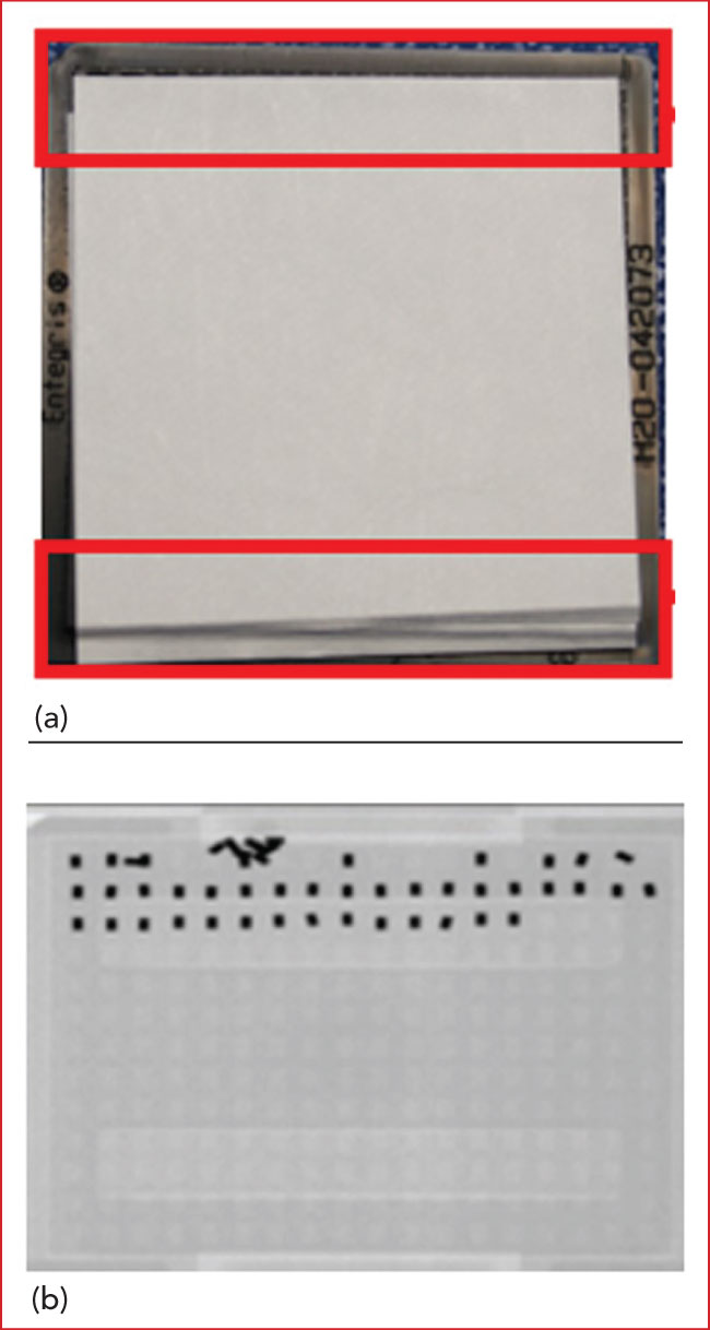
Fig. 4 Misaligned, pinched polyethylene inserts in a waffle pack (a) create openings for COOP (b).penings for COOP (b).
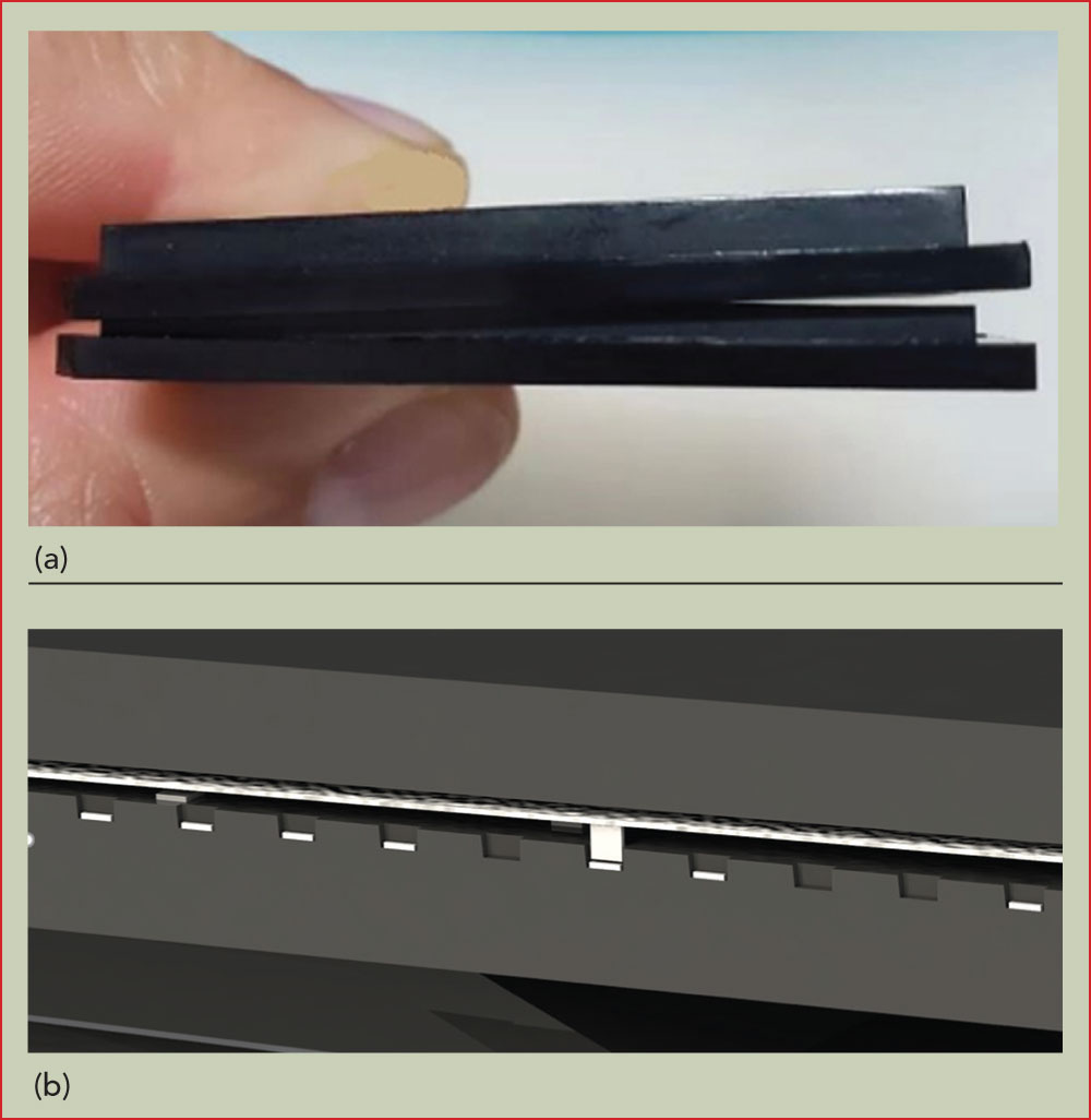
Fig. 5 Waffle pack lid separating from the tray during normal handling (a), leading to COOP (b).
NEW PACKAGING SYSTEM
To prevent COOP, a bare die packaging system needs to encapsulate the die from when the supplier packs the waffle pack, through shipping and unpacking by the customer. As the traditional waffle pack system was designed in a previous era, when devices were much thicker, a simple fix or insert is unlikely to solve the tolerance, quality and structural deficiencies for the current die. To protect the increasingly expensive die they contain, a new packing system is necessary, one compatible with automated manufacturing. The key requirements of a reimagined lid-clip system are
- Captivate the die fully during packing, shipping and unpacking,
- Compensate for waffle pack tray and lid flatness variation within their specified limits
- Use an integrated industry interleaf with no additional modifications, materials or steps
- Provide enhanced electrostatic discharge (ESD) protection, using low outgassing and static dissipative silicone-free materials meeting all relevant industry standards
- Compress the lid uniformly around the full perimeter of the package.
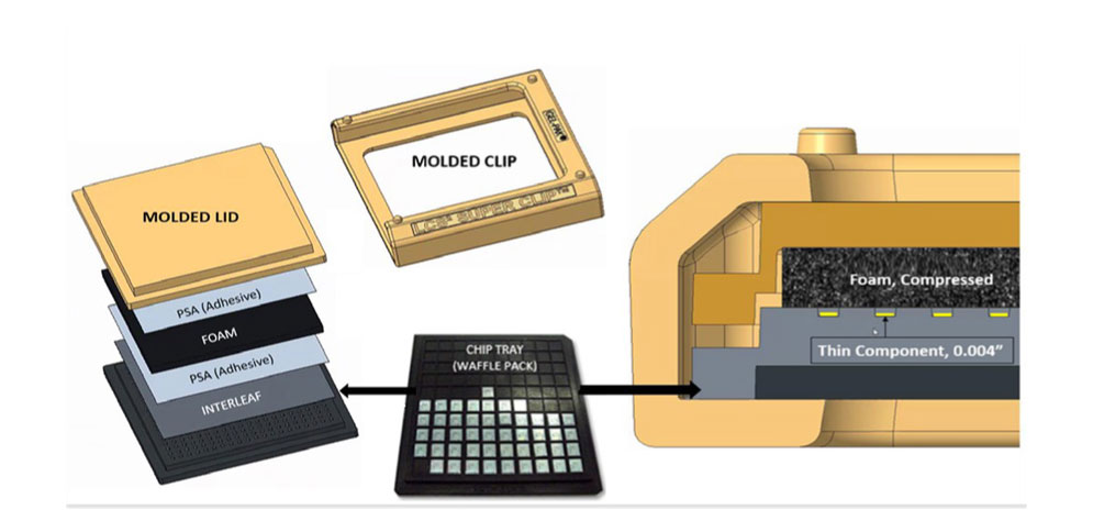
Fig. 6 Structure of the Gel-Pak LCS2 with gasketed tray pockets.
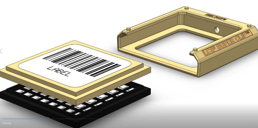
Fig. 7 LCS2 components
TESTING THE LCS2
Testing the LCS2 has demonstrated its efficacy to protect thin semiconductor die. Drop test experiments using several lid-clip combinations and 0.002 in. thick GaN die were conducted, using a 34 in. height to represent catastrophic handling. X-rays verified the security of the die and whether COOP occurred. 100 drop tests were performed on 10 of the lid/clip products. The results showed no COOP (see Figure 9a). When the same test was performed using the historic industry clip instead of the new clip, COOP was observed (see Figure 9b). This test establishes the effectiveness of the new clip design.
Gel-Pak’s LCS2 Super System has demonstrated the capability to virtually eliminate COOP for all sized components, especially ultra-thin die less than 10 mils. The LCS2 reduces non-value-added supplier corrective action requests and return material authorizations. Though the new packaging system must be field tested, the evidence points to LCS2 eliminating millions of dollars in yield loss and improving supplychain quality and efficiency.
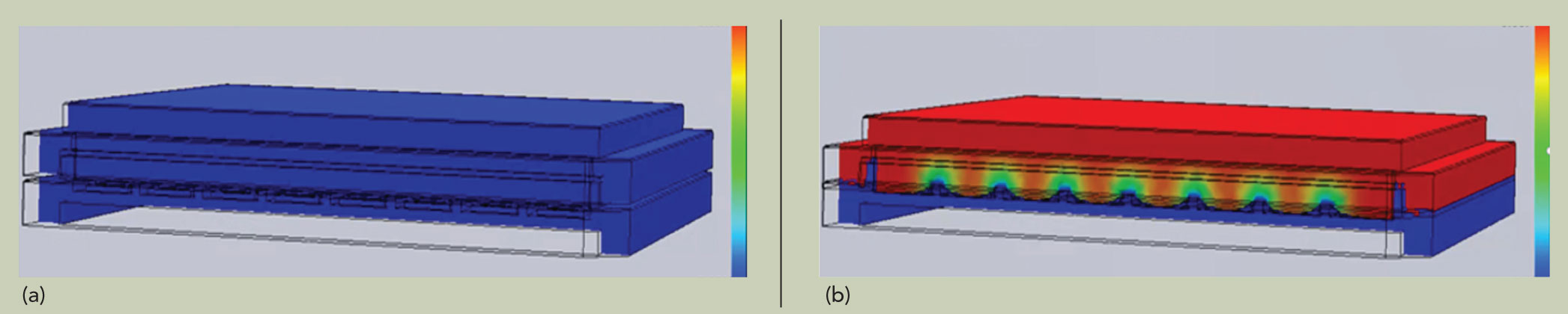
Fig. 8 LCS2 lid on the waffle pack tray without the new clip compressing the foam gasket (a) and with the clip compressing the foam (b). Simulation courtesy of Forgione Engineering.
References
- M. Marks, Z. Hassan and K.Y. Cheong, “Ultrathin Wafer PreAssembly and Assembly Process Technologies: A Review,” Critical Reviews in Solid State and Materials Sciences, 2015, pp. 1–40.
- P. Wadhwani and S. Yadav, “Thin Wafer Market Size,” Report ID: GMI5007, Global Market Insight, March 2021.
- Thinning Equipment Technology and Market Trends for Semiconductor Devices: Market and Technology Report, Yole Développement, 2020.
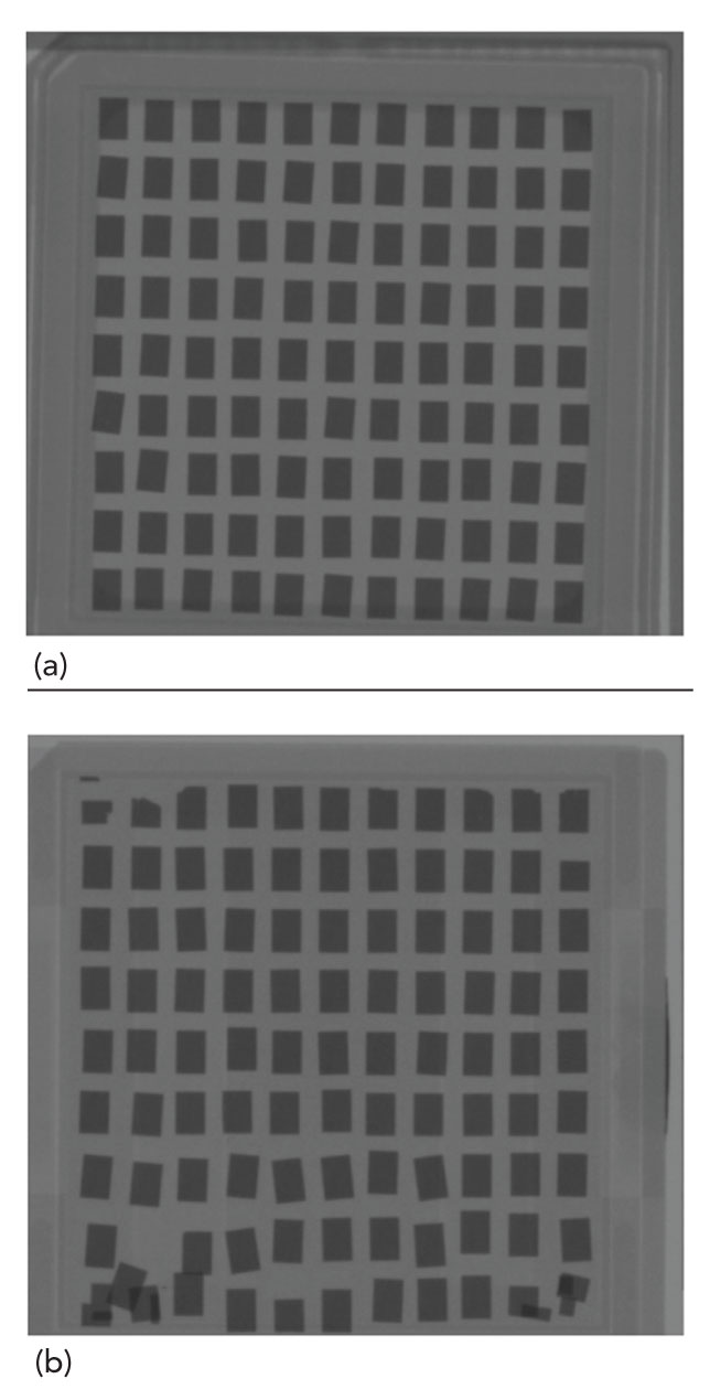
Fig. 9 X-ray images following 10 drops from 34 in. height: LCS2 (a) and new lid with the old industry standard clip (b), the latter leading to COOP and damaged die.